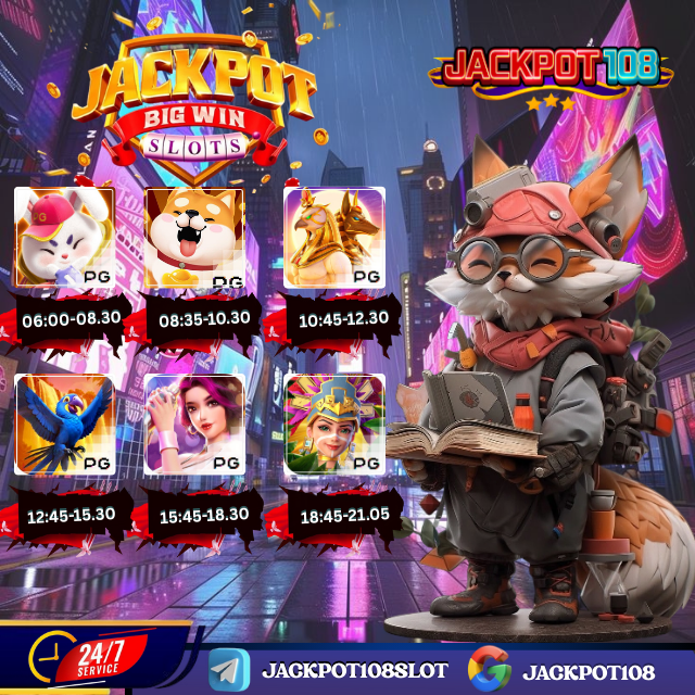
Explore

@ the heart
of Silicon Valley

How Samsung Semiconductor is leading tech innovation and making the connected devices of tomorrow possible.

The best and brightest minds come to Samsung Semiconductor's Silicon Valley campus to develop products that will change how we interact with the world and shape our future.

Over 1200 employees work at Samsung Semiconductor in Sales & Marketing, R&D, and Strategy & Innovation teams. Our Semiconductor division is focused in five main business areas: Memory, Foundry, Display, LED, and System LSI (S.LSI).

The products developed by Samsung Semiconductor are used by world leaders in mobile, automotive, virtual reality / augmented reality (VR/AR), smart wearables, Internet of things (IoT), artificial intelligence (AI), and are enabling unprecedented growth in hyperscale datacenters.

It's now almost a given that each year Samsung Semiconductor will develop and release new products and processes that will shatter previous performance barriers, enabling the next wave of innovation. Right now SmartSSD, 256GB DDR4 RDIMM, and 7nm LLP EUV process technology have the industry buzzing.

Our blueprint
for innovation

How investing in people has made Samsung Semiconductor an unrelenting industry leader.

Every employee at Samsung Semiconductor, from engineers to support staff to marketing, has a role to play in creating the right atmosphere to foster innovation. The new Samsung@First campus was designed around that idea.

With unrestricted views from almost anywhere in the building - employees have more frequent discussions and impromptu, spur-of-the-moment interactions that are the genesis of many great ideas and bonds between our employees.

A healthy work/life balance is paramount to being productive. Our campus is equipped with a Chill Zone, full gym, volleyball and basketball courts, putting greens, bocce ball, table tennis, pool tables, nap pods (zzz), @First cafeteria (yum!), and beautiful green spaces.

Samsung Semiconductor is committed to improving the lives of others and building a better community through fundraising events, charitable donations, beautification projects, and education initiatives.

Powering the
future

We don't just imagine the impossible.
We dare to create it.

Our vision for a future where new technology improves our lives and expands our understanding of the world (and beyond) has less to do with revenue and more to do with advancing humankind in big and impactful ways.

Technological breakthroughs are all in a day’s work for Samsung Semiconductor. It’s a mindset. It’s a belief that faster, smaller, more energy efficient memory, drives, and processors are always possible, even when others say it can’t be done.

Automotive

Datacenter

IoT

AI

When we deliver a new product, we’re helping to drive growth in some of the fastest growing technology sectors: Automotive, data centers, hyperscalers, IoT, and artificial intelligence.

Connecting your
digital world

How Samsung Semiconductor technology is driving a connected revolution and a new way of life.

CONNECTING
YOUR VEHICLE

We’re working closely with our automotive partners to deliver richer and safer in-vehicle experiences while developing groundbreaking new driverless technology to help make autonomous vehicles a reality.

Samsung Automotive DRAM, processors, image sensors, Modem/RF, and eStorage can be found powering ADAS and connected cars all over the world. And we’re one of only a few with an in-house FAB (fabrication) shop, capable of producing custom solutions for top automakers.

ACCELERATING
YOUR LEARNING

Samsung memory enables some of the most sophisticated AI and Machine Learning applications in the world. In this new era of supercomputing, Samsung technology is leading us into a brave new future.

Samsung’s newest High Bandwidth Memory (HBM Aquabolt) delivers record-setting 1.2 terabytes-per-second data transmission rates (10x faster than GDDR5) while reducing power consumption by 20%. It’s staggering to think what this will mean for AI and Machine Learning.

POWERING
YOUR SERVERS

The demand for data processing is exploding and Samsung DRAM, SSDs, and HBM Aquabolt are doing the heavy lifting in data centers everywhere.

We’re focused on maxing out key performance metrics like bandwidth, speed, energy efficiency, and data security. During peak traffic times, our data center customers rely on us to process massive amounts of data, and we don’t like to disappoint. :-)

GROWING
WITH YOU

Our infrastructure and manufacturing capabilities make us one of the only companies in the world that can support the rapid expansion of hyperscale data centers.

Samsung global
leadership

How our relentless pursuit of new technology has made Samsung Semiconductor a fixture on the world stage.

36K+

EMPLOYEES HOLD
DOCTORATE /
MASTERS DEGREES

35

R&D CENTERS
WORLDWIDE

$15B

YEARLY R&D BUDGET

6TH

MOST VALUABLE
GLOBAL BRAND

25%

STAFF IS DEDICATED
TO R&D

$33M

DAILY INVESTMENT

#1

14 AND 10NM FINFET
MASS PRODUCTION

#1

EXYNOS SOCs
MANUFACTURED ON
14NM FINFET

#1

MARKET SHARE IN TV,
SMARTPHONE,
REFRIGERATOR,
LARGE FORMAT
DISPLAY
MONITOR, AND
MEMORY (DRAM,
NAND, SSD)

$17M

IN TECHNOLOGY
INVESTED IN STEM
EDUCATION

#2

MOST REPUTABLE
TECH COMPANIES
(2016)

#1

IN MEMORY (DRAM,
NAND, SSD)

$30M

RAISED FOR
SAMSUNG HOPE FOR
CHILDREN (EST 2002)

100K+

GLOBAL PATENTS

$15.5B

TOTAL INVESTMENT

36

CES 2018
INNOVATION AWARDS

$223B

ANNUAL REVENUE

#2

MOST INNOVATIVE
COMPANIES IN IOT

321K

EMPLOYEES IN 73
COUNTRIES

#3

MOST VALUABLE
BRAND

#21

LINKEDIN TOP
COMPANIES WHERE
PROFESSIONALS
MOST WANT TO
WORK ACROSS THE
U.S. (2018)

#1

OLED AND FLEXIBLE
OLED SUPPLIER

#26

WORLD’S MOST
REPUTABLE
COMPANIES (2018)

1st

PATENT HOLDER IN
THE US (76 ACTIVE PATENTS)

A brief history
of firsts

How Samsung Semiconductor has helped draw the technology curve (1974-present).

1974
Acquisition of Hankook Semiconductor
1974
Wafer Fabrication Begins
1983
64KB DRAM
1987
SSI Opens in Silicon Valley (Then Called Tristar Semiconductor)
1989
SSI Opens the First Semiconductor FAB Outside of Korea
1990
SSI Launches into Global DRAM Market With 1Mb DRAM
1992
64MB DRAM / 250MB Hard Disk
1992
Ranked World’s top DRAM supplier
1994
SSI Expands its HQ
1994
256 MB DRAM Developed
1995
First LCD Screen
1996
1GB DRAM Developed
1996
World's Fastest CPU
1996
#1 in SRAM - First Synchronous Pipelined Burst SRAM
1997
World's Largest LCD
2000
512MB DRAM Developed
2005
World's First OLED
2006
World's First 50nm 1GB DRAM
2006
#2 Design Patent Holder in the US
2007
World's First 30nm Class 64 GB NAND Flash Memory
2009
World’s First 40nm class DDR3 Production
2010
512GB SSD Utilizing DDR NAND
2010
World’s First 30nm class DDR3 Production
2011
Winner of the Innovations Awards at CES
2011
World’s First DDR4 developed
2012
First 3D NAND Flash Memory Chip
2012
World’s First 2GB LPDDR3 production
2013
World’s First 128GB V-NAND1 Production
2013
World’s First 1 TB MSATA SSD
2013
World's First 3D V-NAND Flash Technology
2014
World’s First 8GB DDR4 / LPDDR4 Developed
2015
World's Largest Density Drive - 16TB
2015
World's Fastest SSD
2015
#1 Design Patent Holder in the US
2016
World's First 8GB LPDDR4 Mobile DRAM Package
2016
Samsung Develops 14NM Production Capability
2017
World’s First 256GB V4 Production
2017
1TB NAND Package - Largest Capacity NAND 64 Layer 3-bit 512GB with V4
2017
Worlds’s First 2nd-Generation of 10nm Class 8GB DDR4 DRAM
2017
World’s First Embedded Universal Flash Storage (eUFS)
2017
World's First 15μs Z-NAND SSD
2017
World's First 1TB V-NAND with QLC Technology
2018
World’s Largest Capacity Serial Attached SCSI (SAS) SSD
2018
World’s First 16GB GDDR6 Memory
2018
Samsung Develops SmartSSD
2018
World’s First 256GB DDR4 RDIMM
2018
Samsung Announces 7nm LLP EUV Process
1970s
1980s
1990s
2000s
2010s
Beyond

What's next
@first?

A look ahead at Samsung Semiconductor future tech and a better, digitally enriched tomorrow...

Faster
Processing

Leveraging a new Gate-All-Around transistor structure at 3nm, we’re redesigning SOCs from the ground up to achieve the perfect balance of speed and efficiency.

Advanced
Memory

Pushing the limits of speed and capacity to develop faster flash memory and storage for next-gen devices, applications, and infrastructure.

Reduced
Form Factors

Decreasing device footprints to enable innovations in mobile, bioprocessor, IoT, datacenter, automotive, and beyond.

Increased
Storage Density

Charting the course beyond 1TB NAND as we continue to redefine industry standards for reliability, security, and endurance.

FASTER
TIME TO INSIGHT

Bringing processing power directly to the SSD itself with SmartSSD, drastically reducing data movement while accelerating lightweight computing.

Ultra
Low Latency

Accelerating flash performance with new circuit and controller design for latency-sensitive, I/O-intensive applications like high capacity caching, NoSQL databases, data stores, and business analytics.

Improved
Energy Efficiency

Our relentless drive to reduce power consumption means more cost-effective and environmentally friendly devices.

LEADING
EUV LITHOGRAPHY

Reducing design and production cycle times for high-performance, low-power SoCs from months to weeks with proprietary 7LPP EUV process node technology.

SMARTER
CONNECTED DRIVING

Preparing for the ADAS driving revolution with our super-fast '5G-ready' telematics system built for today’s 4G networks and future 5G networks.

FUTURE
DISPLAY TECH

Opening up new frontiers for smartphones and VR with future display tech like Infinity Flex Display, Aqua Sensor, Sound on Display (SoD) and GD Glass (1200 ppi).

Take the next
step with us

Do you have something special to contribute?
Learn more about working at Samsung Semiconductor in Silicon Valley.

@ The Heart Of Silicon Valley
Our Blueprint For Innovation
Powering The Future
Connecting Your Digital World
Samsung Global Leadership
A Brief History Of Firsts
What's Next @first?
Take The Next Step With Us